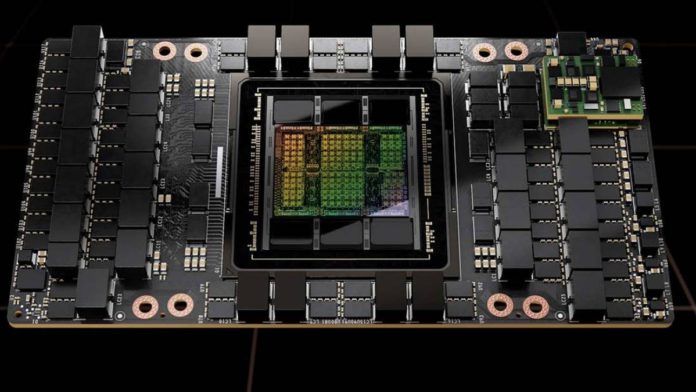
NVIDIA is driving more and more architectural decisions and modifications in its CPU and GPU accelerator engines with each new generation. Jensen Huang, CEO of NVIDIA, announced that the company would ramp up Hopper, an architecture supporting AI workloads. The Hopper architecture is intended to scale diverse workloads for data centers.
NVIDIA unveiled Hopper in March, along with other advancements like the NVIDIA Grace CPU. This month, the company released benchmark results for the chip in the MLPerf suite of machine learning tasks.
Hopper is built with approximately 80 billion transistors with NVIDIA’s cutting-edge TSMC 4N technology and features multiple innovations to enhance the performance of NVIDIA H100 Tensor Core GPUs.
Read More: NeMo LLM Service: NVIDIA’s cloud service to make AI less complicated
The company has pushed the H100 Tensor Core GPUs to enter the production zone in total volume. The GPU chips will be shipped to companies including Hewlett Packard, Dell, Cisco Systems, etc. NVIDIA systems with the H100 GPU will enter the market in the first quarter of next year.
When the company launched the first H100 GPU chip, Huang said, the chips would be “the next generation of accelerated computing.” The H100 chip is designed to accomplish artificial intelligence tasks for data centers. The company claims that H100 chips “dramatically” reduce deployment costs for AI-based programs. For instance, the performance of 320 top-of-the-line A100 GPUs is equivalent to only 64 H100s.


