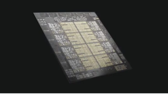
It is not uncommon that microchips and processors have contributed to the immense development of artificial intelligence-based applications. In recent years, chip developers have been partaking interest in designing AI-based chips to further the usage of artificial intelligence. Not only that, given the acute crisis in the semiconductor industry, the manufacturers are also looking forward to improving the efficiency of AI-based chips. This is why IBM and Samsung are working on the IBM Telum microprocessor, which has a specifically designed architecture for AI activities. The chip is reported to be available in the first half of 2022.
Dubbed as the next-generation CPU for IBM z and LinuxONE systems, IBM gave a sneak peek of IBM Telum chip during IEEE’s recent Hot Chips 33 conference.
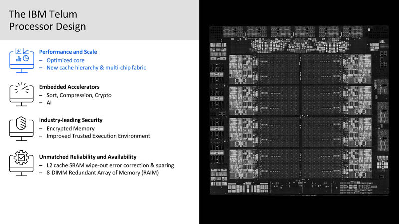
The Telum processor has eight CPU cores, on-chip task accelerators, and 32MB of semi-private cache, according to IBM. Each chip module will include two Telum dies that are closely linked for a total of 16 cores per socket. To give you an idea of how unusual this design is, the previous z15 CPU had twelve cores and a separate chip for a shared cache. In addition, the Telum CPU will be made on a Samsung 7nm Extreme Ultraviolet Lithography (EUV) technology, rather than the 14nm process utilized for the z15 chip. According to IBM, the chip represents the initial involvement of the IBM Research AI Hardware Center.
The new chip, according to a subsequent press release, is intended to aid in the detection of fraud in real-time.
According to IBM, the concept for such a processor arose from a market study that revealed 90% of businesses wish to be able to build and run AI projects regardless of where their data is stored. Telum is built to accomplish precisely that, allowing businesses to execute high-volume inferencing for real-time critical transactions without relying on off-platform AI solutions that might slow down operations by impacting performance speeds.
The chip, as per IBM, features a deep superscalar out-of-order instruction pipeline with a clock frequency of more than 5GHz, making it ideal for heterogeneous enterprise-class workloads. This is crucial because calculations in CPUs of classical computing systems are executed by constantly relaying data and instructions between the memory and processor, while AI workloads have significantly greater processing requirements and operate on enormous amounts of data. To allow very low-latency AI inference, a heterogeneous system consisting of CPU and AI cores tightly integrated on the same chip is a must.
The practice of feeding live data points to machine/deep learning models in order to create the desired result is known as AI inference. It is the second step of the AI lifecycle, with training being the first — so without training, AI inference may be challenging. When AI inference is performed outside of the system where data is stored, it can result in low throughput and high latency. This is primarily why businesses are often late in discovering security and fraud issues.
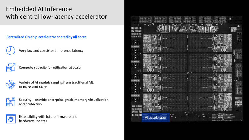
In the IBM Telum, the AI inference is made possible by processing real-time input data locally on the machine where data is being hosted. This AI accelerator uses a mix of the Open Neural Network Exchange standard (ONNX) and IBM’s proprietary Deep Learning Compiler to run models created with a range of mainstream AI frameworks.
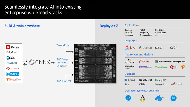
In simpler words, IBM Telum allows AI inference while processing data. This enables businesses to include deep learning models into their transactional workloads, allowing them to not only acquire insights from data during the transaction but also to use those insights to influence the transaction’s outcome. The AI accelerator has an inferencing performance of six teraFLOPS, which can be expanded up to a 32-chip mainframe with a performance of 200 teraFLOPS. So no more long waits for verifying if your card transaction is fraudulent or not.
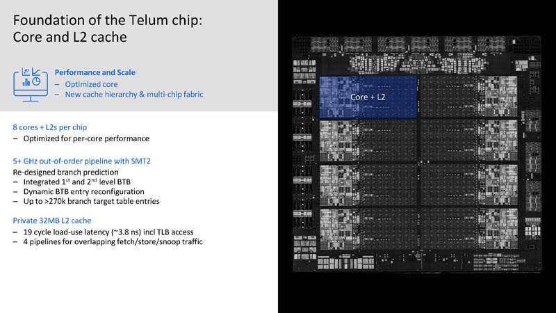
Each core in IBM Telum chip includes a dedicated L1 cache and 32MB of low-latency “semi-private” L2 cache. Because the L2 caches are combined to create a shared virtual 256MB L3 across the cores on the chip, it is referred to as “semi-private.” For communications, the L2 caches are connected through a bi-directional ring bus with a bandwidth of over 320 GB/s and an average latency of just 12ns. The L2 caches are also employed to develop a shared virtual L4 cache amongst all of the chips in a drawer. Each drawer has up to four sockets and two processors, for a total of eight chips and 64 CPU cores, as well as 2GB of shared L4 cache.
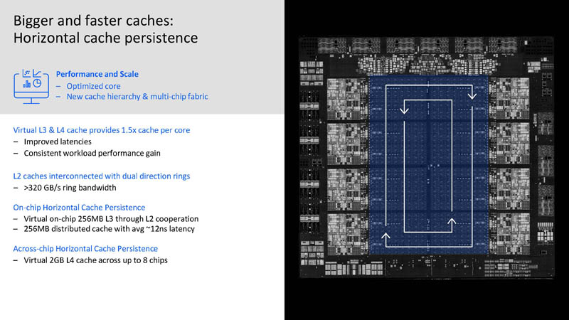
The new cache and chip-interconnection technology provides 32MB cache per core and can extend to 32 Telum chips.
Along with processor core enhancements, the 1.5x increase in cache per core over the z15 generation is designed to provide a considerable boost in both per-thread speed and overall capacity delivered by IBM in the next generation IBM Z system.
Read More: Latest AI Model From IBM, Uncovers How Parkinson’s Disease Spreads in an Individual
According to IBM, the newly optimized Z core, in combination with its brand new cache and multi-chip fabric architecture, allows for a performance increase of over 40% per socket.
As per the IBM newsroom blog, Telum also offers important security advancements, such as transparent main memory encryption. Its Secure Execution enhancements are designed to improve speed and usability for Hyper Protected Virtual Servers and trusted execution environments, making Telum the perfect solution for sensitive data processing in Hybrid Cloud architectures. Other key advancements in Telum include a redesigned 8-channel memory interface capable of tolerating complete channel or DIMM failures and transparently restoring data without affecting response time.
For more info watch:


